
Design / Finetune
PCB layout & design
Translate a schematic into a board ready for manufacturing review. Layout starts with electrical intent, mechanical constraints and a clear set of design rules.
Discuss this service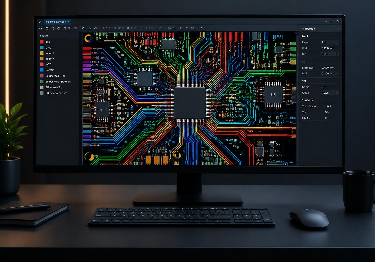
Project scope
Built around your requirements.
These are areas to discuss in your brief. Final scope, feasibility and timing depend on your specific design and requirements.
- Component placement and routing
- Multilayer board layout
- Mixed-signal and high-speed requirements review
- Manufacturing file preparation
Before we begin
What to share.
- 01Schematic and component libraries
- 02Board outline and mechanical constraints
- 03Layer stack-up and routing requirements
- 04Fabricator rules and required output formats
A clear handoff
Agree the outcome.
Agree editable source files, Gerber and drill outputs, assembly data and design-review checkpoints before layout starts.
What files are needed to start PCB layout?
Start with a schematic, bill of materials and board dimensions. Share component footprints, connector positions, stack-up requirements and any impedance or clearance constraints. If these are not final, identify the open decisions first.
Process / Design
From requirements to an agreed handoff.
Establish design constraints
Identify the schematic revision, component libraries, board outline, mounting points and fixed connector locations.
Agree placement and routing rules
Discuss stack-up, clearance, impedance and signal requirements alongside the selected fabricator’s rules.
Define review and file release
Agree placement and routing checkpoints, output formats and the editable source files needed for handoff.
Deliverables to agree
Define what changes hands.
- Editable design-source formats to agree
- Gerber and drill file requirements
- Assembly data and design-review checkpoints
Quality review
Make acceptance specific.
Set the review method and evidence required for these project-specific checks.
- Footprints and placement against the schematic and BOM
- Routing constraints against agreed design rules
- Board outline, mounting and connector alignment
Scope boundaries
Layer count, routing complexity, high-speed requirements and tool formats need confirmation. Layout review does not replace prototype validation, EMC testing or product certification.
Common questions
Before you enquire.
Does layout include schematic design?
The layout brief starts with a schematic. If circuit design is still needed, separate that work from layout and discuss the engineering scope first.
Which manufacturing files will I receive?
Agree Gerber, drill, assembly and editable source formats before work starts. Required files depend on the fabricator, assembler and design tools selected for the project.
Related services
Your next build